Electronic – bjt (common-collector configuration) – valuable tech notes Pnp common base circuit diagram [solved]: 1. draw the schematic diagram of the fol
Pnp And Npn Circuit Diagram - 4K Wallpapers Review
Pnp transistor circuit diagram What is common collector connection (or cc configuration)? Common collector configuration circuit diagram
Pnp transistor tutorial
Introduction to pnp transistorBjt- emitter follower (common collector amplifier) explained with Pnp transistor introduction diagram circuit bjt working electronic engineeringIntroduction to transistors.
Pnp common collector circuit diagramCommon collector connection Différences entre les transistors npn et pnp et leur fournisseur uniqueFigure configuration amplifier.
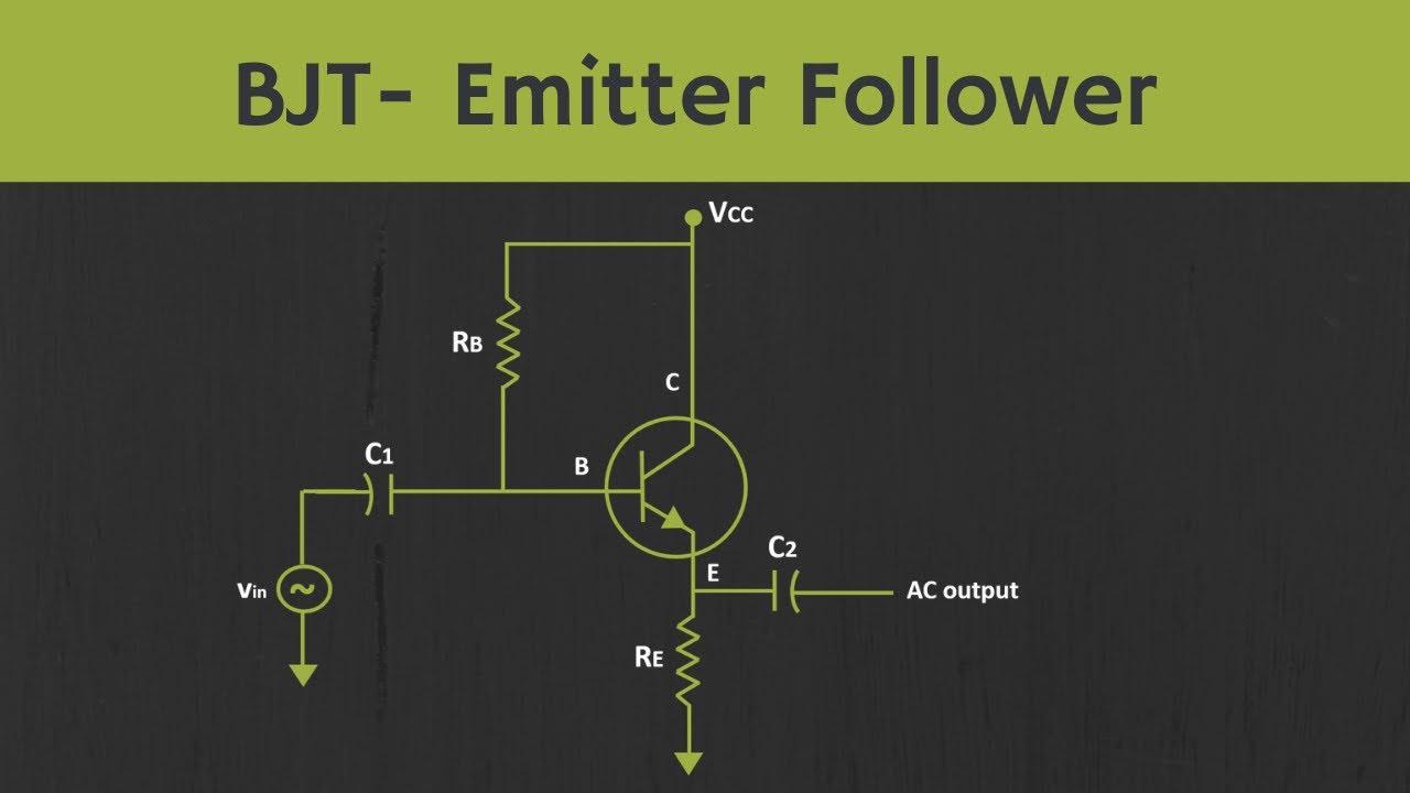
Cc amplifier circuit diagram
Circuit diagram for pnp transistorCircuit diagram of cb configuration for pnp transistor Figure: common collector circuitCommon emitter (ce) configuration.
Pnp transistor circuit diagramPnp transistor transistors types circuit basics diagram current modes npn advantages working electronics components active mode electronic use do collector Emitter follower bjt collector amplifierCommon collector transistor circuit diagram.

Pnp and npn circuit diagram
Pnp and npn circuit diagram26 transistor characteristics modern lab experiments documentation Solved q3 common-collector amplifier (pnp) for the circuitHow to design a transistor amp in common-collector configuration with.
Common collector configuration circuit diagramCommon collector amplifier circuit Collector current transistor npn amplifier circuit pnp circuitglobe amplificationCommon emitter pnp transistor circuit diagram.

Pnp common collector circuit diagram
.
.


Cc Amplifier Circuit Diagram

How to design a transistor amp in common-collector configuration with

Solved Q3 Common-collector amplifier (pnp) For the circuit | Chegg.com
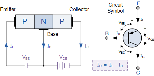
PNP Transistor Tutorial - The Bipolar PNP Transistor

Introduction to Transistors - Types, Baising Modes and Advantages

Pnp And Npn Circuit Diagram - 4K Wallpapers Review

Introduction to PNP Transistor - The Engineering Projects

Common Emitter (CE) Configuration - SUNTEC CAMPUS TUTORIAL
